EE 322
Phase-Locked Loops (PLL's) and PM Demodulation
The purpose of this lab is to use a phased-locked loop circuit
to implement a simple demodulator for frequency modulated signals.
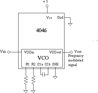
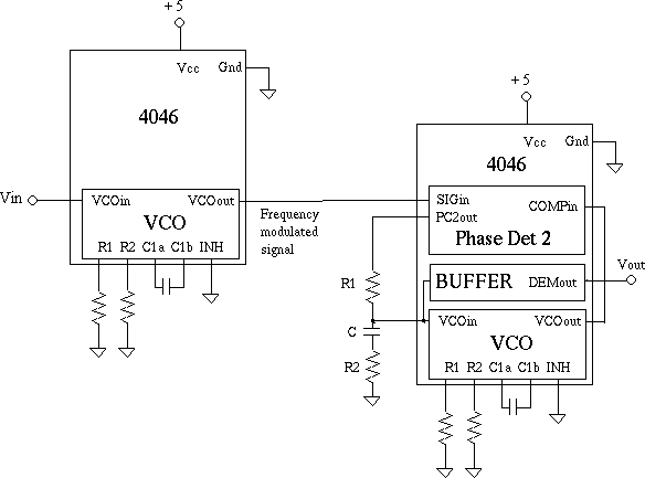
Use two 4046 chips in this lab, the first will produce a FM signal using
only the VCO portion of the chip. The second will be a PLL to demodulate
the signal.
WARNING -- there are two different chips in the lab, 4046A and 4046B. They are different
and require different Rs and Cs. There is a data sheet for each.
Voltage-Controlled Oscillator
Phased-locked loops are available in integrated-circuit packages
which contain a phase-detector and a VCO. The PLL we will use
in the lab is the popular 4046. The VCO frequency range for
the 4046 is determined by two external resistors and an external
capacitor. The discussion on the 4046 in the correct data sheet
shows how to select values for these components.
- Design the VCO part of the PLL to have a frequency range of
10 kHz centered around a carrier frequency of 50kHz.
- Build the VCO portion of the PLL. Verify that the with 1 V
in, the VCO frequency is at its minimum frequency, and with 4 V
in, the frequency is at its maximum (use 5 V for Vcc). You may have to fiddle with
the values of R1 and R2 to get good results.

- Build and test a second VCO on another chip with the same components.
Adjust the components to make the frequency range the same for both.
Phased-Locked Loop
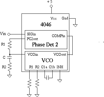
To use the PLL as a demodulator, we need to finish the PLL by
adding the phase detector and low-pass filter. The 4046 has
three different phase detectors, as discussed in the data book.
For this experiment, we will use the Type~2 detector. We will
also use a simple RC filter as the low-pass filter, as discussed
in class.
- Add the low-pass filter to the output of the
phase detector. As discussed in class,
choose your components so that w0 is about the highest
frequency in your modulated signal, 100 Hz. Choose Q = 0.7.

- Connect the output of the low pass filter to the input
of the VCO. Connect the output of the VCO to the
Comparator In pin of the 4046. Set up your function generator
to generate a square wave from 0 V to 5 V at 50 KHz. Connect the output
of the function generator to the Signal In pin of the PLL 4046.
Verify that the PLL works; i.e., verify that the output frequency
of the VCO is the same as the input frequency from the function
generator for frequencies near your carrier frequency. What are
the maximum and minimum frequencies the PLL can lock onto?
- What is the phase difference between the two signals going
into the phase comparator for different input frequencies?
- What is the (average) input voltage to the VCO for different
input frequencies?
- Sketch and explain the output of the Phase Comparator II Out
pin.
PM demodulation

- Connect the signal generator to your frequency modulation circuit
(the other VCO). Set the
generator to produce a 100 Hz sinusoid with an offset and amplitude
which will produce maximal frequency shifts.
- Connect the VCO modulator
to the PLL input.
- Observe the output of the PLL 'DEMODULATION OUT'. How is it related
to the output of the signal generator?
- Increase the frequency of the
sin input and find the highest frequency that the modulation
can be recovered.
- Change the input to a 100 Hz square wave. Sketch the resulting step
response of the system. Is it what you expected?
© Copyright 1997 New Mexico Institute of Mining and Technology
