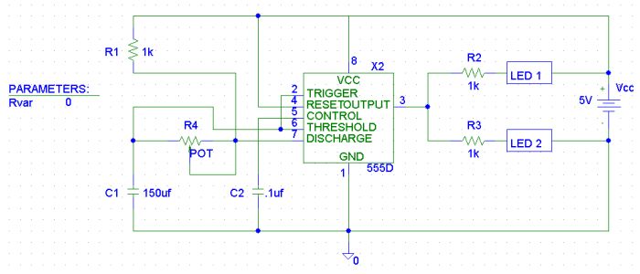
 Figure 1
EE 101
Lab Exercise 6: The 555 Timer
For this lab, you will use PSPICE to simulate your design, and to verify that your design is valid. It is absolutely critical that you get a working design today, because this schematic will be used later to generate a printed circuit board for your final project. Settling for a non-working design today will result in constructing a non-functional final project!
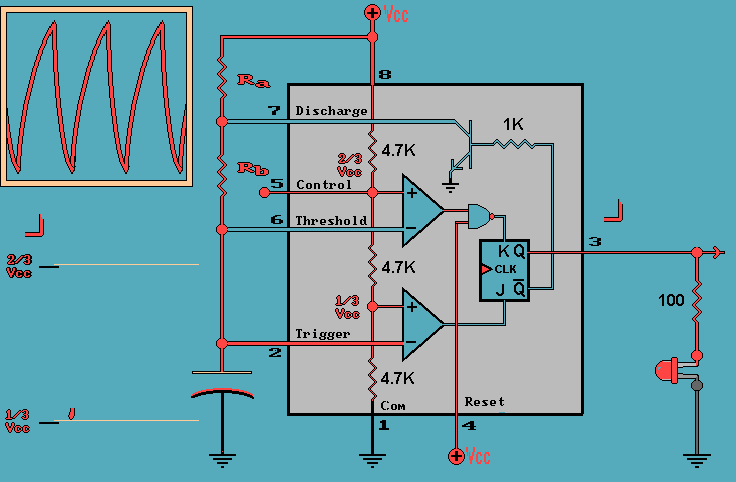
Here is a great annimation of the 555 timer operation. Definitely check this out and see if you can correlate the annimated behavior with the material we covered in the prelab lecture. [Complements of Rensselaer Polytechnic Institute www.rpi.edu]
Part I - Entering your schematic in PSPICE
- If you haven't already done so, finish the calculations in the last step of the prelab.
- Using the PSPICE schematic capture program, enter the schematic that you designed in the pre-lab. Refer to Figure 1 to help you with parts placement and attributes. Parts of the schematic in Figure 1 are deliberately left out. These items are left for the student to put in. (The 555 timer and diodes are located in the eval library and the potentiometer is located in the breakout library).
- The part name for the variable resistor is POT. Under attributes, you will need to define its package type. Ask your instructor which potentiometer we are using this semester, the package type will either be TO-39 or TO-220AB. You will also need to define its value as {Rvar}. The brackets around this name allow for you to designate the potentiometer's value as a changeable parameter, and you must type the brackets around the Rvar.
- LED's are not defined PSPICE's libraries. For these parts, use the diode D1N4148. Rename the D1 and D2 designators LED1 and LED2. Make sure you orient them correctly in your schematic.
- To simulate the changing value of the potentiometer, you will use a feature in PSPICE named "parameters". To set this up, first add the part "PARAM" (located in the special library) to your schematic. Place the parameters block to the side of your schematic. Edit the parameters attributes as follows:
- Name1 = Rvar
- Value1 = 0
- Under the Analysis menu, choose setup and configure the following:
- Bias Point Detail - make sure this is selected
- Parametric - Swept Variable Type = Global Parameter
- Sweep Type = linear
- Name = Rvar
- Start Value = 0
- End Value = 10K
- Increment = 1K
- Transient - Print Step = 0.1s
- Final time = 3s
- Be sure to connect the power supply (+ 5VDC), ground, and a voltage marker to your circuit.
- Print a copy of the schematic diagram for your lab book (By this time we shouldn't have to tell you this right? It's a critical part of documenting your experiment.) For printing, it helps to select a rectangular area around the schematic with the mouse, in the print dialog, select "print only selected area" and scale it to 100%. This number can be changed to control the size of the printout.
Below are some items to help you define certain elements of your circuit:
- Perform an electrical rule check on your circuit. If this reports any errors, fix them at this time.
-
Simulate your design (shortcut it F11 key). After several seconds of calculations, the Probe
Window will pop up with a smaller window in front of it.
- In this smaller window are the ten settings for Rvar. All are selected at first.
- Deselect all of them by clicking on "None."
- Select the Rvar = 0 setting with your mouse (it should be at the top of the list) and click on "OK."
- A waveform will appear.
- Using the cursors, measure the period of this waveform and calculate its frequency. It will be a little tricky here because the low portion of the waveform is very short, you can use the magnifier to zoom in if needed.
- Verify that this frequency is close to what you calculated (it should be in your pre-lab data).
- Print a copy of the waveform (remember to print four plots per page for a good printout size).
- To check how your circuit reacts with different values of Rvar, repeat step two above, each time trying different values for Rvar. Use 3 KΩ, 6 KΩ, and 10 KΩ.
- Compare all results (for each case of Rvar equaling 0, 3K, 6K, and 10K) to those you calculated in the pre-lab and print out the waveforms for each.
- Extra Credit: Observe the high vs. low portions of the waveform for each Rvar value.
- Are they symmetrical (does the duration of the high portion equal the duration of the low portion)? Does this affect the frequency of the signal?
- When you repeat this process for the other Rvar values, how does the hi/lo proportion compare as frequency changes?
- Is this a problem for a digital TTL application? (A digital TTL system is triggered by either rising or falling transitions between high and low values.) Explain why or why not.
September 2006 | © 2001, New Mexico Tech