EE 101
Lab Exercise 9: Printed Circuit Board Artwork Generation
In Phase I of the class project (lab 6), you designed and simulated a circuit that would alternately flash two LED's while outputting a TTL compatible waveform adjustable from about 1Hz to 10Hz. In Phase II (lab 7) you prototyped your design on a breadboard and enhanced it to provide outputs over several other frequency ranges. In Phase III, you will scale back your design to theoriginal specifications from lab 6 and generate artwork which will create a printed circuit board (PCB). Your design should be similar to theone in Figure 1.
There are some extremely important things to keep in mind for this lab:
- It is absolutely imperative that you have a working circuit before you move ahead with
this lab. We are about to design the physical layout of your design, so if your circuit is
not currently working properly, you will build a non-working circuit. If you had simulation
trouble in lab 6, or any other problems that suggest your circuit is not 100% correct, we
need to fix that NOW, or your finished product will not work.
- You can not assume your circuit is identical to the example diagrams in these
instructions. There are certainly some significant differences between your schematic and
the one that generated these images. Therefore you will need to identify your equivalent
components by figuring out what they are connected to, rather than using the labels. DO NOT simply match up your labeled components to the same labels on the diagrams here, this will certainly generate an incorrect layout.
- Similarly, do not rely on p-spice to have transfered your labels from the schematic to the pcboard view properly. Do not assume that the labels on your schematic correspond to the same labels in the rats nest. Again, be certain which component is which by identifying what they are connected to rather than by their labels.
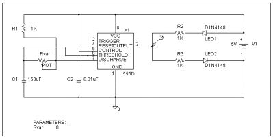 Figure 1
Converting your schematic to a PC Board
- Execute the MSIM Schematics program.
- Open your design file from Lab 6, and save it under a new name (Click File - Save As) in your account.
- Take a few minutes to verify that each circuit element (R's, C's, diodes, the potentiometer, and the 555) has a package type defined for it.
- From the Tools menu, select Run PCBoards. The
Microsim PCBoards program willstart and the netlist from your design will be loaded (see
Figure 2). Theremay be some warnings or errors reported with your netlist. Warnings are
generally OK, but if you get any errors you will have to give them attention before proceeding.
Figure
2
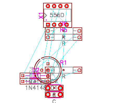
Rats Nest Layout
Figure 2 shows a jumbled mess of your components and their footprints (package types). The light blue lines connecting all of these are called the "rats nest." You will be responsible for placing these footprints in such a way that they can be connected together
easily.
First you will draw a component "keep in" border.
The Board Signal Keepin is a rectangle, shown in Figure 3, which will define the size of your printed circuit board.
- Go to the Draw menu and select Board Signal Keepin. The grid spacing on the desktop is measured in mills (thousandths of an inch), with the default being that each dot is 50 mills apart.
- At the lower left of the screen are two numbers reported in mills, which report the cursor position on the screen. Make the rectangle 2.0" wide (2000mills) and 1.9" high (1900 mills) around the components and rats nest, as shown in Figure 3.
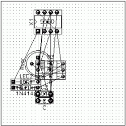
Figure 3
Next you will move each component to a proper position
within the keepinlayer.
- Use Figure 4 as a guide. Do not assume that the part labels on
this drawing correspond to your part labels. For example, your R1 may not be the same resistor as R1 in the drawing, so confirm the parts in your schematic before matching to this figure.
- Move each part by selecting it with the mouse and dragging it to its proper place.
- Rotate parts (Ctrl+R) as necessary, but do not flip sides or mirror any footprints. This could result in your artwork not matching your schematic.
- Keep in mind that, depending on which kind or potentiometer we use this semester, yours may look different in this diagram. This one shows the TO-39 footprint, if you used the TO-220
footprint your pot will show up as a rectangular shape with three in-line pads instead of the circular one shown here.
- Make sure you leave enough space around each component so that the parts will fit on your board when you solder them on. Remember that the 150uF capacitor is larger than Pspice thinks, and the POT is about twice the size as the footprint you see on screen.
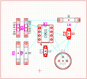
Figure 4
Editing the Solder Layer
Next we will begin editing the image that will create your actual PC board. What you see on screen is a combination of several layers. We are trying to design the copper layer for soldering on your board, so the changes we make should be on the Solder Layer. Other layers display helpful information such as labels and component footprints, but when we print the layout onto a copper board, we only want to use the solder layer.
- Click on the Board Layer field box on the toolbar (it
probably is set for "Component")
- Change the board layer to Solder.
The first editing you need to do is to enlarge the solder pads. These are where we will drill holes and solder the wire leads of the components to the PC board. Be very careful not to accidentally delete a pad in this stage. The only way to replace a deleted pad is to start over with a new rats nest!
- Select each component pad (the placewhere the component
leads go through the board) by double clicking on the center of the pad. This should bring up an attributes window for the selected pad.
- Select PIN_PADSTACK and set the value to (rnd or sq)-080-040. This will size all of the pads so that their outer
diameter is 80 mils and they will all have a 40 mil hole in the center.
- Pads that are already square should have the "sq" designation, and round pads should be "rnd." The shape of the pad is an orientation indicator so do not change the shape of a pad.
Now, by following the connections shown in the rat's nest, you will draw the actual connections, or traces, of your design. These are the flat copper 'wires' on your pc board that will connect your components together.
- Click on the Trace Style field box on the toolbar and
select Trace_50. This will automatically set the width of your traces to 50 mils.
- From the Draw menu, select Trace. (Ctrl+T). This works like a line-drawing tool.
- Use the crosshairs to draw the connections between the connected nodes in the rat's nest. Use Figure 5 as a pattern, but remember you can not copy it exactly, you must follow the connections needed on YOUR PCB. As you replace the necessary connections indicated by the thin light-blue lines with your thick blue trace line, the indicator lines should disappear. If they do not, be sure you're drawing the proper connection and that the traces extend fully to the center of the pad. Sometimes you need to delete a trace section and redraw it for PSpice to notice the connection.
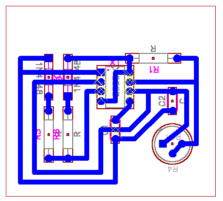
Figure 5
We will add some labels to your drawing by using the Draw-Text menu option.
- Add your name (and class and date if you want to) to your board.
- Once the text is placed, select it by lassoing it with the mouse.
- Select the Edit-Mirror option to reverse it. Later when you iron your artwork transfer onto a copper board, your name be reversed again and appear readable.
- With your text still selected, click on the Font size field and select a larger font (text_100 is a good size).
Now you need to add copnnection points on your board to attach your VCC (+5V)and Ground inputs.
- Identify a good location for these connection points
- As shown in Figure 6, draw traces to where the VCC and ground pads will be located (make sure to do this on the solder layer).
- Add the pads (Draw - Component - Jump1). An "X" will appear where you have added your new connections. This indicates that the two traces touching at that point do not have the same name. Normally, this would be a cause for concern, but not this time. Ignore the "X's".
- Add text blocks for VCC and GND and mirror them, as shown in the figure. Be sure you label them with the correct name by following them back to something you know connects to GND or VCC.
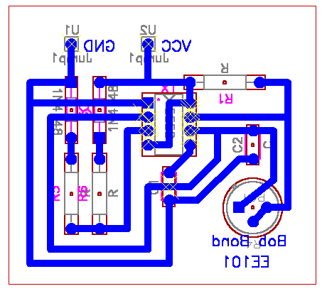
Figure 6
In order to have your artwork print out properly, your entire design needsto be moved to a specific area on the desktop.
- Select your entire designby lassoing it with the mouse.
- Move the selected area so that the lower-left corner of the block is at grid location 2400, 3700. This way, your designshould print out near the center of the page. At other locations, it may not print out at all.
Printing Instructions
Read carefully, If you don't follow these instructions you will end up printing out mountains of useless wasted paper!
- DO NOT simply click the Print button on the toolbar
- Select Print from the File menu.
- Click on Job Setup.
- In the field where all the page numbers are listed, delete all page numbers except number 1. If you do not do this, many wasted pages will print out when we execute the print command.
- Click on the 1 (page 1) to highlight it. Several board layers will be listed in the field to the side.
- Select Solder Layer and Board Sig Keepin layers only. This will print your artwork exactly as it will transfer onto your PCB.
- Click on OK
- Check the Black and White box and 1 to 1.
- Print the job.
For reference, you should also print the circuit again showing the components this time. Go back to the job
setup screen and add these layers to page 1 (in addition to the solder and keepin layers): Boundary Top, Assembly Top, Silk Top, Mask Top, and Component. Now print the job again and
put both of these images in your lab book.
The rest of this experiment will be during the etching session that each of you must schedule! Your instructor will have a sign-up sheet for individual etching sessions. Be sure you sign up and show up on time. This project takes a significant amount of your instructor's time, so if you miss it or show up late you may not be able to reschedule. The etching session should take about three hours. Before this session you must familiarize yourself with the process by going through the presentation in Lab 13.
March 2006© 2002 New Mexico Tech